Xradia has released a new element-specific x-ray imaging tool for semiconductor metrology, scanning electron microscopes, and electron probe micro analyzers.
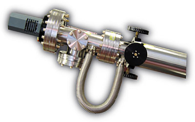
The nanoXFi x-ray fluorescence imager collects and images fluorescence x-rays characteristic of elements that emit them when exposed to x-ray and electron beams. The nanoXFi images the spatial distribution of an element of interest in the sample, resolving feature sizes smaller than 100nm. Nearly all elements of the periodic table can be imaged in this manner. The first application of the nanoXFi is in semiconductor manufacturing, using electron beam excitation to characterize production wafers in semiconductor wafer fabs.
The fluorescence imager also attaches to scanning electron microscopes and electron probe micro analyzers, providing users with powerful new imaging capability, allowing non-destructive element-specific imaging inside samples of interest.
Resulting images are obtained by exploiting the ability of electron and x-ray beams to penetrate below the surface of the sample and produce element-specific fluorescence images that contain depth information.
"X-ray fluorescence imaging allows for the visualization of complex structures, one element at a time, in the domain of tens of nanometers," said Xradia founder Dr. Wenbing Yun . "This is a potent new tool for nanotechnology, biotech, and semiconductor manufacturing with the potential to revolutionize the field of microscopy," observed Bill Diamond of Xradia. The nanoXFi is currently in production and shipping to initial OEM customers.
Xradia develops high-resolution nondestructive x-ray imaging products for nanometer resolution 3D pictures of complex objects and element-specific views for process control and monitoring in IC manufacturing.